PCB Design

With years of experience, PrototipX's talented engineers design the PCB designs you need in accordance with production standards and today's technology.The electronic design process works like this:
- Creating/Editing Electronic Diagrams
- PCB Layout Drawing
- Mechanical CAD Design
- Control and Test Procedures
- Verification and Confirmation Processes
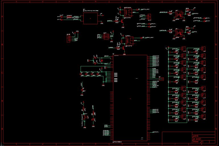
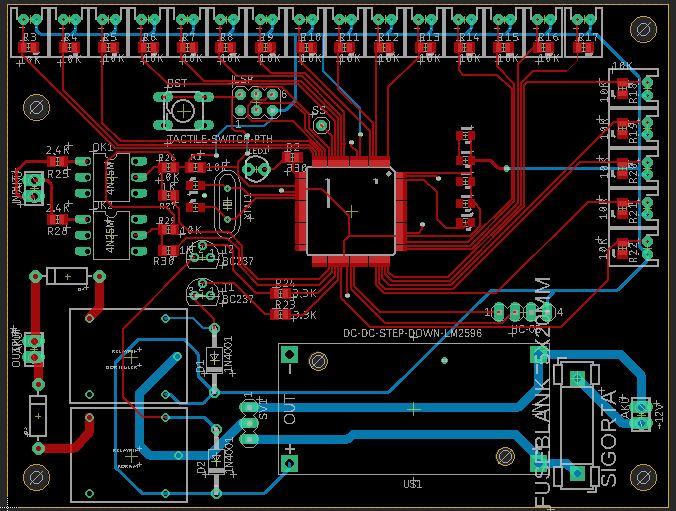
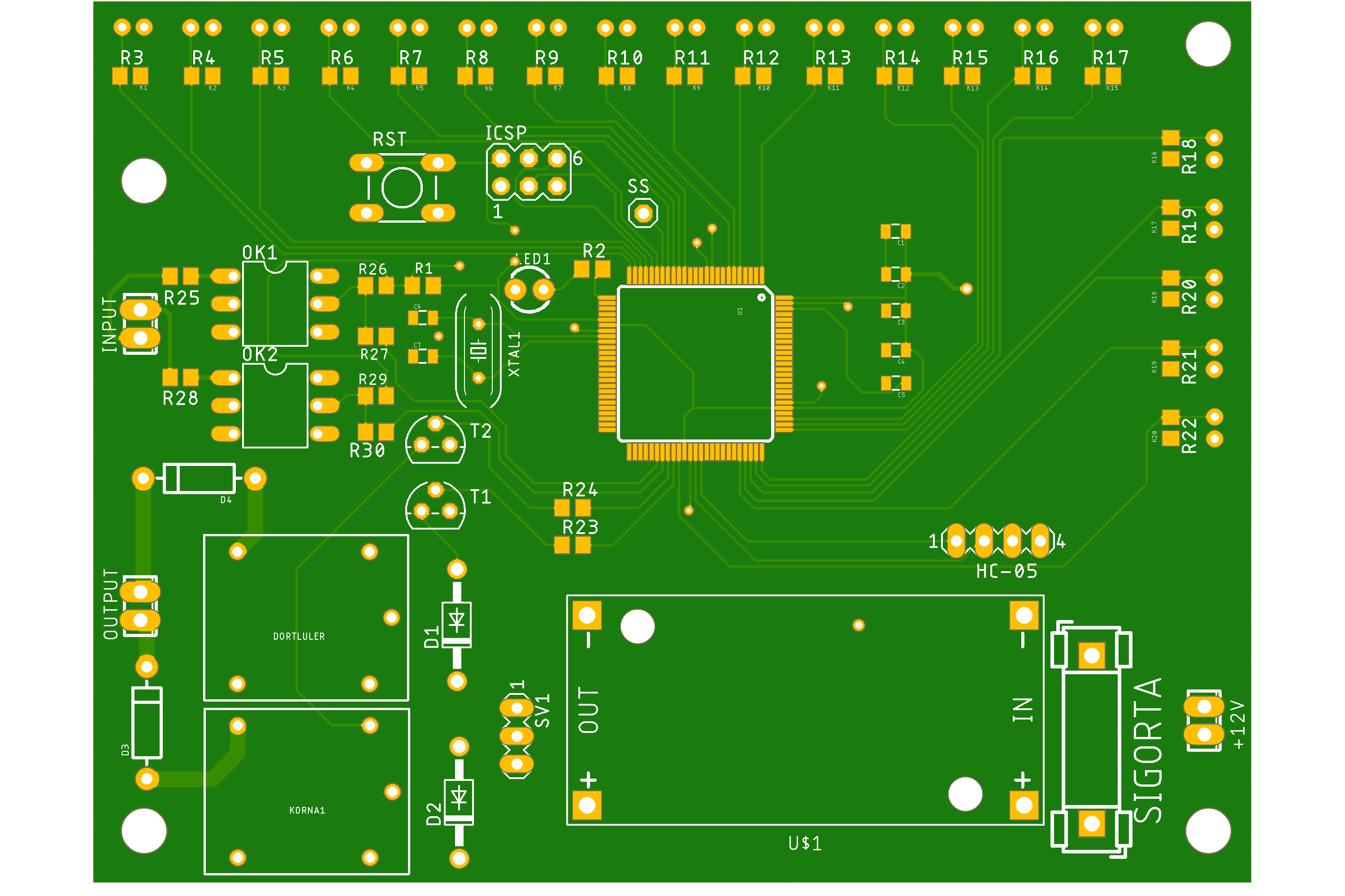
The electronic schematic may be created by the customer as well as by our engineers. This issue is an important parameter as per our pricing policy. The electronic diagram must contain basic information such as the package type of the components used by a technical person, electrical connection paths, current calculations.Transferring the data of the electronic schematic to the PCB Layout is a fundamental issue. Criteria such as design dimensions, technical details, component sheath types are taken into account. PCB Layout work is done in accordance with the criteria. The PCB Layout is revised again, taking into account the update requests for the current product. The data that the production will need is created and archived.
Creating Electronic Diagrams
We create the electronic diagrams of the equipment you need with appropriate component covers. In the development process, we act in accordance with the principles and standards of electronic circuit design.
PCB Layout Drawing
After the prepared circuit diagram, the board design, electrical connection paths and components are placed. After this stage, the PCB is designed with the current to be carried by the roads, the number of layers and the desired Board dimensions.
GERBER File
After the completion of the board design, you can either produce it with prototypeX or you can produce from anywhere with the GERBER file delivered to you.
PCB and file submissions at the end of the design are as follows:
- Transferring the company logo onto the PCB
- Creation of BOM and parts lists
- Generating the GERBER file
- PCB's technical documents